|
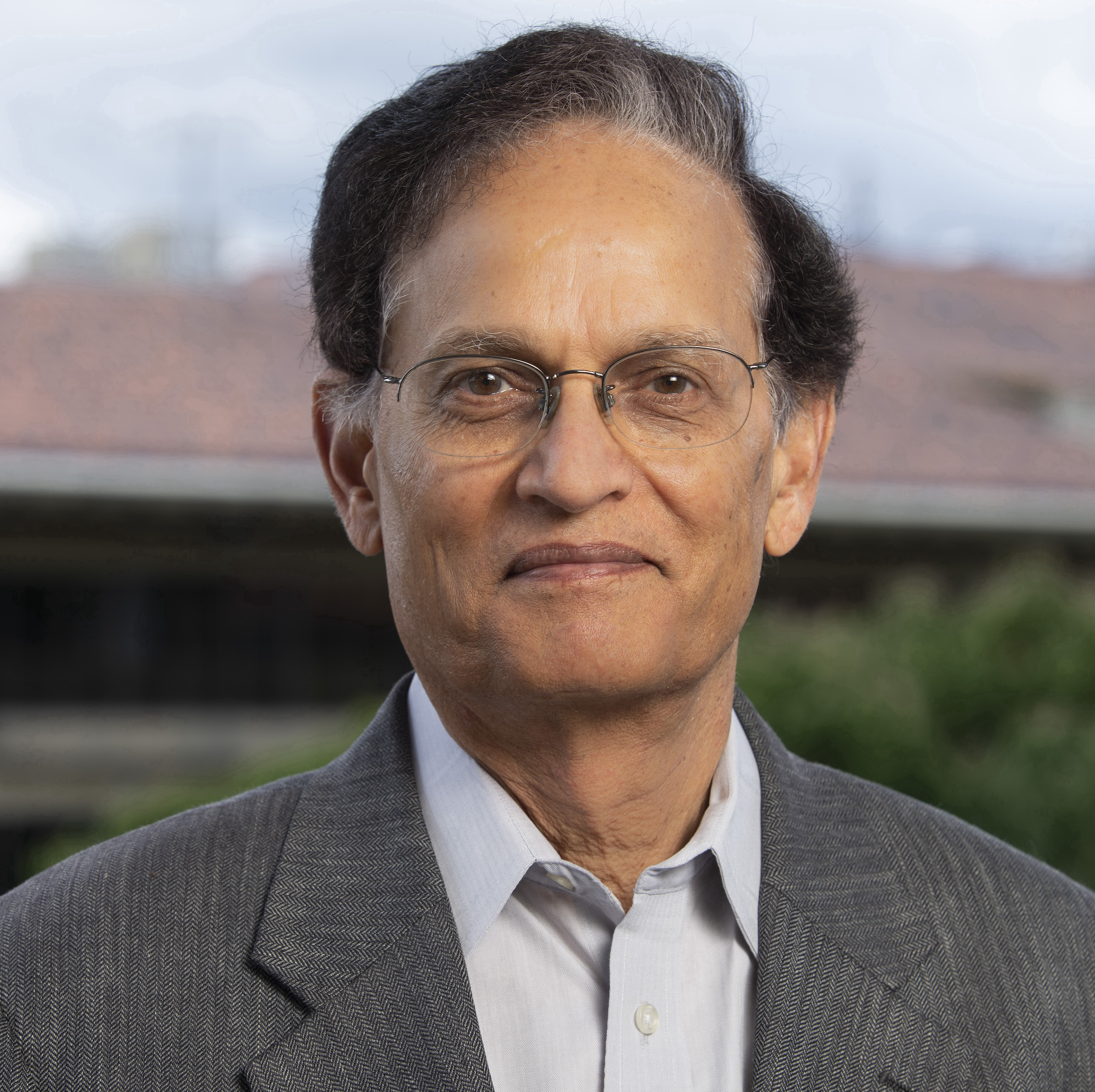
Krishna Saraswat
|
|
|
|
||
|
Prof. Saraswat received his B.E. degree in Electronics in 1968 from the Birla Institute of Technology and Science, Pilani, India, and his M.S. and Ph.D. degrees in Electrical Engineering in 1969 and 1974 respectively from Stanford University, Stanford, CA. Professor Saraswat stayed at Stanford as a researcher and was appointed Professor of Electrical Engineering in 1983. He also has an honorary appointment of an Adjunct Professor at the Birla Institute of Technology and Science, Pilani, India since January 2004 and a Visiting Professor during the summer of 2007 at IIT Bombay, India. During 2000-2007 he was Associate Director of the NSF/SRC Center for Environmentally Benign Semiconductor Manufacturing. He has been a technical advisor, board member and consultant to several industrial organizations in USA, Asia and Europe. He has also advised several academic and government organizations world wide. Professor Saraswat's research interests are in new and innovative materials, structures, and process technology of semiconductor devices and interconnects for nanoelectronics and solar cells. During 1969-70, he worked on microwave transistors at Texas Instruments. Returning to Stanford in 1971, he did his Ph.D. on high voltage MOS devices and circuits. After graduating he joined Stanford University as a Research Associate in 1975 and later became a Professor of Electrical Engineering in 1983. For the next 15 years, he worked on silicon semiconductor fabrication technology. He pioneered the technologies for aluminum/titanium layered interconnects, CVD of tungsten and tungsten silicide MOS gates. During the late 80Õs he became interested in the economics and technology of single wafer manufacturing. He developed equipment and simulators for single wafer thermal processing, deposition and etching and technology for the in-situ measurements and real-time control. Jointly with Texas Instruments a microfactory for single wafer manufacturing was demonstrated in 1993. Since the mid 90Õs he has been working on new materials, devices and interconnects for nanoscale MOSFETs and solar cells. He has pioneered several new concepts of 3-D ICs with multiple layers of heterogeneous devices. His group demonstrated the first high performance germanium CMOS and III-V antimonide CMOS with metal gate and high-k dielectrics. His current research is on new device structures and materials to improve solar cell efficiency and lower cost, continue scaling MOS transistors and semiconductor memories to nanometer regime, 3-dimentional ICs with multiple layers of heterogeneous devices, and optical interconnections. Prof. Saraswat has supervised close to 100 doctoral students, 40 research scholars and has authored or co-authored 15 patents and over 850 technical papers, of which 10 have received Best Paper Award. He is a Life Fellow of the IEEE. He received the Thomas Callinan Award from The Electrochemical Society in 2000 for his contributions to the dielectric science and technology, the 2004 IEEE Andrew Grove Award for seminal contributions to silicon process technology, Inventor Recognition Award from MARCO/FCRP in 2007, the Technovisionary Award from the India Semiconductor Association in 2007, BITS Pilani Distinguished Alumnus Awards in 2012, the Semiconductor Industry Association (SIA) Researcher of the Year Award in 2012, and the Semiconductor Research Corporatin (SRC) Aristotle Award in 2021. He is listed by ISI as one of the Highly Cited Authors in his field. |
||